GOKTUG
All Logic Gates Verilog VHDL and ModelSim Codes
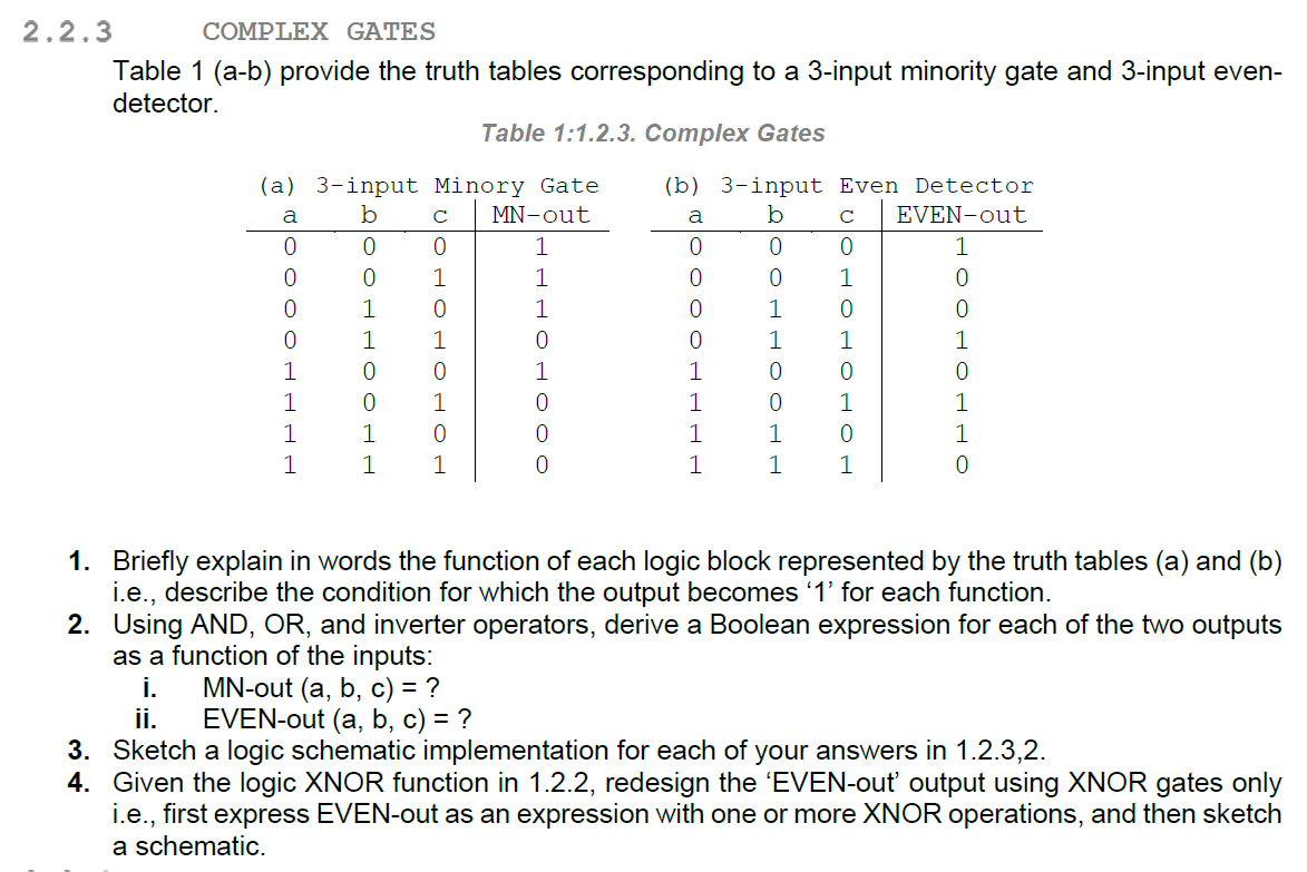
Complex Gates Verilog VHDL and ModelSim Codes
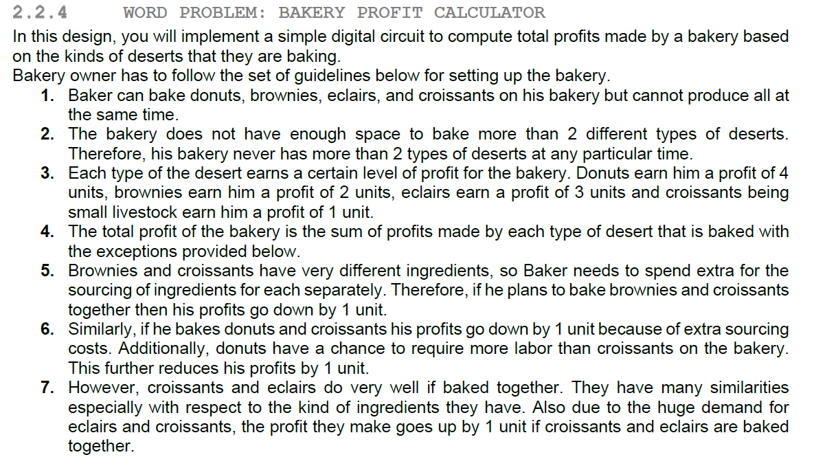
Bakery Profit Calculator Verilog VHDL and ModelSim Codes
Adder/Subtractor Verilog VHDL and ModelSim Codes
Comparator Verilog VHDL and ModelSim Codes
Decoder Verilog VHDL and ModelSim Codes
Full Adder Verilog VHDL and ModelSim Codes
Ripple Carry Adder Verilog VHDL and ModelSim Codes
Arithmetic Unit Verilog VHDL and ModelSim Codes
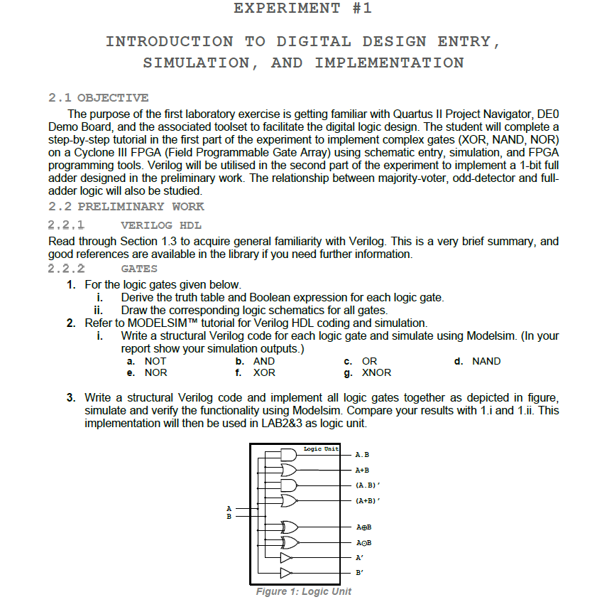
Logic Unit Verilog VHDL and ModelSim Codes
Arithmetic Logic Unit Verilog VHDL and ModelSim Codes
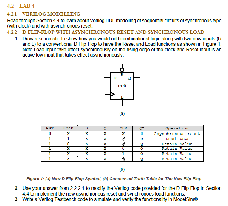
D Flip-Flop Verilog VHDL and ModelSim Codes
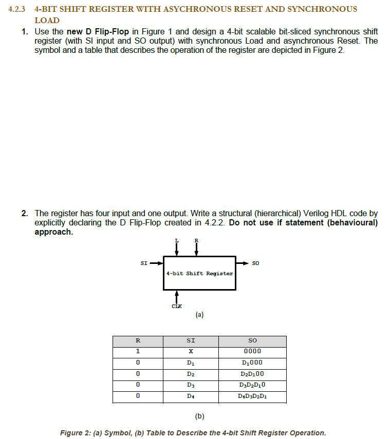
Shift Register Verilog VHDL and ModelSim Codes
Up-Down Counter Verilog VHDL and ModelSim Codes
Down Counter With D-Type FF Verilog VHDL and ModelSim Codes
Down Counter With JK-Type FF Verilog VHDL and ModelSim Codes
Paralel Load Shift Register Verilog VHDL and ModelSim Codes
Fibonacci Series Calculator Verilog VHDL and ModelSim Codes
Fibonacci Series Datapath Verilog VHDL and ModelSim Codes
FSM Design Verilog VHDL and ModelSim Codes